Genesis:32X Service Bulletin Fixes: Difference between revisions
(Since Asian VA4s use the same board as European units, they are affected by this as well) |
|||
| (5 intermediate revisions by the same user not shown) | |||
| Line 2: | Line 2: | ||
== Overview == | == Overview == | ||
The service bulletins detail three fixes for the model 1. Two are specifically for the VA4 revision of the PAL Mega Drive and one is for the VA5 and its sub-variants (VA6, 6.5 and 6.8). The latter fix applies to all regions and not just PAL consoles. | The service bulletins detail three fixes for the model 1. Two are specifically for the VA4 revision of the Asian and PAL Mega Drive, and one is for the VA5 and its sub-variants (VA6, 6.5 and 6.8). The latter fix applies to all regions and not just PAL consoles. | ||
The two fixes for the PAL VA4 concern the EDCLK (external dot clock) and VCLK (68000 clock) signals, which in stock form are not "clean" enough for the 32X. Sega found that as the Mega Drive warmed up to room temperature, the EDCLK signal would gradually become unstable, causing screen elements rendered by the 32X to jitter until the 32X locked up. This can often take up to an hour to manifest. Similarly, Sega discovered that the VCLK signal on the VA4 would also cause the 32X to lock up. The EDCLK signal can be improved by substituting C92 with a 33 pF capacitor, removing both ferrite bead FB7 and capacitor C112, and adding a jumper wire. The VCLK signal can be improved by simply removing two capacitors, C78 and C100. | The two fixes for the Asian/PAL VA4 concern the EDCLK (external dot clock) and VCLK (68000 clock) signals, which in stock form are not "clean" enough for the 32X. Sega found that as the Mega Drive warmed up to room temperature, the EDCLK signal would gradually become unstable, causing screen elements rendered by the 32X to jitter until the 32X locked up. This can often take up to an hour to manifest. Similarly, Sega discovered that the VCLK signal on the VA4 would also cause the 32X to lock up. The EDCLK signal can be improved by substituting C92 with a 33 pF capacitor, removing both ferrite bead FB7 and capacitor C112, and adding a jumper wire. The VCLK signal can be improved by simply removing two capacitors, C78 and C100. | ||
On the VA5, 6, 6.5 and 6.8, the quality of the VCLK signal can also cause the 32X to lock up. This is rectified by removing capacitor C78 and adding a jumper wire between its topmost pad and pin 15 of the 68000 CPU, which is the clock input. | On the VA5, 6, 6.5 and 6.8, the quality of the VCLK signal can also cause the 32X to lock up. This is rectified by removing capacitor C78 and adding a jumper wire between its topmost pad and pin 15 of the 68000 CPU, which is the clock input. | ||
| Line 22: | Line 22: | ||
* Desoldering braid (optional) | * Desoldering braid (optional) | ||
== Procedure for PAL VA4 == | == Procedure for Asian/PAL VA4 == | ||
# Flip over the Mega Drive and remove the six screws securing the case. Carefully pull off the top case and remove the connector on the power LED itself. You may need to straighten out the LED leads with a pair of needlenose pliers as they are typically bent over. | # Flip over the Mega Drive and remove the six screws securing the case. Carefully pull off the top case and remove the connector on the power LED itself. You may need to straighten out the LED leads with a pair of needlenose pliers as they are typically bent over. | ||
#* Do ''not'' remove the power LED on the motherboard end as the connector is soldered directly to the board. | #* Do ''not'' remove the power LED on the motherboard end as the connector is soldered directly to the board. | ||
# Remove the screws for the top RF shield then set the shield aside. After removing the screw underneath the headphone jack PCB, remove the two long screws on each side of the cartridge port and the three long screws on the heat sink. | # Remove the screws for the top RF shield then set the shield aside. After removing the screw underneath the headphone jack PCB, remove the two long screws on each side of the cartridge port and the three long screws on the heat sink. | ||
#* Asian Mega Drive consoles do not have RF shielding but will still have several screws securing the board to the bottom case. | |||
#* Be careful not to mix up these screws or damage to the bottom case will result if you use one of the long screws anywhere else. | #* Be careful not to mix up these screws or damage to the bottom case will result if you use one of the long screws anywhere else. | ||
# Pull the power jack PCB out of the screw boss securing it, then carefully lift the motherboard out of the bottom case. Set the bottom case and RF shield aside. | # Pull the power jack PCB out of the screw boss securing it, then carefully lift the motherboard out of the bottom case. Set the bottom case and RF shield aside. | ||
# Turn the motherboard upside down and locate capacitor C112, which is a disc-type ceramic capacitor soldered between one of the pads for C19 and the board. Desolder it from the board and set it aside. | # Turn the motherboard upside down and locate capacitor C112, which is a disc-type ceramic capacitor soldered between one of the pads for C19 and the board. Desolder it from the board and set it aside. | ||
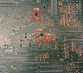
#* See Figure 1 for the location of C112 and the other two capacitors you will remove in the next step. | |||
# Locate capacitors C78 and C100. C78 is a 1206 SMD capacitor around the center of the board while C100 is another disc-type capacitor located below the cartridge port. Desolder both. C78 can be "swept" off the board by loading both its pads with solder and using your soldering iron to heat both points at the same time. Be careful not to bridge the pads. | # Locate capacitors C78 and C100. C78 is a 1206 SMD capacitor around the center of the board while C100 is another disc-type capacitor located below the cartridge port. Desolder both. C78 can be "swept" off the board by loading both its pads with solder and using your soldering iron to heat both points at the same time. Be careful not to bridge the pads. | ||
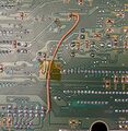
# Solder a wire between the topmost pad of C10 and ground. Ground can be found at many places on the board, but Sega recommended using the middle pad of EM16, which is one of the line filters for controller port 1. | # Solder a wire between the topmost pad of C10 and ground. Ground can be found at many places on the board, but Sega recommended using the middle pad of EM16, which is one of the line filters for controller port 1. | ||
#* See Figure 2. | |||
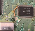
# Flip the motherboard right side up again. Locate FB7, which is a ferrite bead located directly above the master clock oscillator. You can remove it by simply cutting it out or desoldering it. Once it has been removed, jump the points by soldering a small piece of wire or component lead between them. | # Flip the motherboard right side up again. Locate FB7, which is a ferrite bead located directly above the master clock oscillator. You can remove it by simply cutting it out or desoldering it. Once it has been removed, jump the points by soldering a small piece of wire or component lead between them. | ||
# Locate capacitor C92 which is another disc ceramic capacitor and is located near the left side of IC4, the 315-5364 bus arbiter. Desolder it and then solder the 33 pF capacitor you removed earlier in its place. | #* See Figure 3. | ||
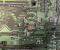
# Locate capacitor C92 which is another disc ceramic capacitor and is located near the left side of IC4, the 315-5364 bus arbiter. Desolder it and then solder the 33 pF capacitor you removed earlier in its place. You may need to use a small length of wire to connect one of the leads of the 33 pF capacitor to one of the pads. | |||
#* See Figure 4. | |||
# Reassemble the system so that it can be tested with a 32X. Make sure to test for at least an hour to ensure that the 32X will not lock up once the Mega Drive has fully warmed up. Once testing has been completed and the 32X is stable, fully reassemble the Mega Drive. | # Reassemble the system so that it can be tested with a 32X. Make sure to test for at least an hour to ensure that the 32X will not lock up once the Mega Drive has fully warmed up. Once testing has been completed and the 32X is stable, fully reassemble the Mega Drive. | ||
=== Gallery === | |||
<gallery> | |||
Image:PAL32XJitter.png|An example of the jitter caused by the PAL VA4's stock EDCLK signal. Note how the main screen, rendered by the 32X, is unstable while the elements rendered by the Mega Drive are perfectly fine. | |||
Image:VA4ClockFix2.jpg|Fig. 1. Remove the three capacitors highlighted in red, but do not discard C112 once it's been removed. | |||
Image:VA4ClockFix3.jpg|Fig. 2. Solder a wire between ground and the top pad of C10 as shown here. | |||
Image:VA4ClockFix1.jpg|Fig. 3. Remove these two components. | |||
Image:VA4ClockFix4.jpg|Fig. 4. The 33 pF capacitor that was previously removed is now soldered in place of C92. A jumper has also been soldered in place of FB7. | |||
Image:PAL32XFixed.png|A VA4 after the service bulletin fixes have been applied. | |||
</gallery> | |||
== Procedure for VA5/6/6.5/6.8 == | == Procedure for VA5/6/6.5/6.8 == | ||
| Line 41: | Line 56: | ||
#* Japanese Mega Drive consoles do not have RF shielding but will still have several screws securing the board to the bottom case. | #* Japanese Mega Drive consoles do not have RF shielding but will still have several screws securing the board to the bottom case. | ||
#* Be careful not to mix up these screws or damage to the bottom case will result if you use one of the long screws anywhere else. | #* Be careful not to mix up these screws or damage to the bottom case will result if you use one of the long screws anywhere else. | ||
# | # On non-Japanese consoles, pull the power jack PCB out of the screw boss securing it, then carefully lift the motherboard out of the bottom case. Set the bottom case and RF shield aside. | ||
# Locate capacitor C78, which is a 1206 SMD capacitor. Remove it by loading both its pads with solder, then use your soldering iron to carefully "sweep" it off the board. | # Locate capacitor C78, which is a 1206 SMD capacitor. Remove it by loading both its pads with solder, then use your soldering iron to carefully "sweep" it off the board. | ||
#* See Figure 1. | |||
# Solder a wire from the topmost pad of C78 to pin 15 of the 68000 CPU, which is the very large chip located directly next to the cartridge port. Make sure that the wire goes around the cartridge port pins and not through them, as the cartridge port support in the bottom shell may crush the wire if you route it through the pins. | # Solder a wire from the topmost pad of C78 to pin 15 of the 68000 CPU, which is the very large chip located directly next to the cartridge port. Make sure that the wire goes around the cartridge port pins and not through them, as the cartridge port support in the bottom shell may crush the wire if you route it through the pins. | ||
#* See Figures 2 and 3. | |||
# Reassemble the system so that it can be tested with a 32X. Make sure to test for at least an hour to ensure that the 32X will not lock up once the Mega Drive has fully warmed up. Once testing has been completed and the 32X is stable, fully reassemble the Mega Drive. | # Reassemble the system so that it can be tested with a 32X. Make sure to test for at least an hour to ensure that the 32X will not lock up once the Mega Drive has fully warmed up. Once testing has been completed and the 32X is stable, fully reassemble the Mega Drive. | ||
== Gallery == | === Gallery === | ||
<gallery> | <gallery> | ||
Image: | Image:VA6ClockFix1.jpg|Fig. 1. Remove C78, highlighted in red. | ||
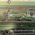
Image: | Image:VA6ClockFix4.jpg|Fig. 2. The clock input pin of the 68000 CPU. | ||
Image:VA6ClockFix3.jpg|Fig. 3. The completed fix. Note how the wire has been routed so it does not get crushed by the cartridge port support in the bottom case. | |||
</gallery> | </gallery> | ||
[[Category:Genesis]] | [[Category:Genesis]] | ||
Latest revision as of 05:41, 4 September 2024
Soon after the 32X's release, Sega became aware of various compatibility issues with the 32X and certain revisions of the model 1 Genesis/Mega Drive. During this time, Sega issued several bulletins to authorized service centers detailing these problems and how to rectify them. All of these fixes involve removing certain components from the Genesis/Mega Drive motherboard and rerouting clock signals.
Overview
The service bulletins detail three fixes for the model 1. Two are specifically for the VA4 revision of the Asian and PAL Mega Drive, and one is for the VA5 and its sub-variants (VA6, 6.5 and 6.8). The latter fix applies to all regions and not just PAL consoles.
The two fixes for the Asian/PAL VA4 concern the EDCLK (external dot clock) and VCLK (68000 clock) signals, which in stock form are not "clean" enough for the 32X. Sega found that as the Mega Drive warmed up to room temperature, the EDCLK signal would gradually become unstable, causing screen elements rendered by the 32X to jitter until the 32X locked up. This can often take up to an hour to manifest. Similarly, Sega discovered that the VCLK signal on the VA4 would also cause the 32X to lock up. The EDCLK signal can be improved by substituting C92 with a 33 pF capacitor, removing both ferrite bead FB7 and capacitor C112, and adding a jumper wire. The VCLK signal can be improved by simply removing two capacitors, C78 and C100.
On the VA5, 6, 6.5 and 6.8, the quality of the VCLK signal can also cause the 32X to lock up. This is rectified by removing capacitor C78 and adding a jumper wire between its topmost pad and pin 15 of the 68000 CPU, which is the clock input.
Materials and Tools
Materials
- Leaded solder
- Flux (optional but highly recommended)
- Hookup wire
Tools
- JIS/Phillips head screwdriver
- Soldering iron
- Flush cutters
- Wire strippers
- Tweezers
- Desoldering braid (optional)
Procedure for Asian/PAL VA4
- Flip over the Mega Drive and remove the six screws securing the case. Carefully pull off the top case and remove the connector on the power LED itself. You may need to straighten out the LED leads with a pair of needlenose pliers as they are typically bent over.
- Do not remove the power LED on the motherboard end as the connector is soldered directly to the board.
- Remove the screws for the top RF shield then set the shield aside. After removing the screw underneath the headphone jack PCB, remove the two long screws on each side of the cartridge port and the three long screws on the heat sink.
- Asian Mega Drive consoles do not have RF shielding but will still have several screws securing the board to the bottom case.
- Be careful not to mix up these screws or damage to the bottom case will result if you use one of the long screws anywhere else.
- Pull the power jack PCB out of the screw boss securing it, then carefully lift the motherboard out of the bottom case. Set the bottom case and RF shield aside.
- Turn the motherboard upside down and locate capacitor C112, which is a disc-type ceramic capacitor soldered between one of the pads for C19 and the board. Desolder it from the board and set it aside.
- See Figure 1 for the location of C112 and the other two capacitors you will remove in the next step.
- Locate capacitors C78 and C100. C78 is a 1206 SMD capacitor around the center of the board while C100 is another disc-type capacitor located below the cartridge port. Desolder both. C78 can be "swept" off the board by loading both its pads with solder and using your soldering iron to heat both points at the same time. Be careful not to bridge the pads.
- Solder a wire between the topmost pad of C10 and ground. Ground can be found at many places on the board, but Sega recommended using the middle pad of EM16, which is one of the line filters for controller port 1.
- See Figure 2.
- Flip the motherboard right side up again. Locate FB7, which is a ferrite bead located directly above the master clock oscillator. You can remove it by simply cutting it out or desoldering it. Once it has been removed, jump the points by soldering a small piece of wire or component lead between them.
- See Figure 3.
- Locate capacitor C92 which is another disc ceramic capacitor and is located near the left side of IC4, the 315-5364 bus arbiter. Desolder it and then solder the 33 pF capacitor you removed earlier in its place. You may need to use a small length of wire to connect one of the leads of the 33 pF capacitor to one of the pads.
- See Figure 4.
- Reassemble the system so that it can be tested with a 32X. Make sure to test for at least an hour to ensure that the 32X will not lock up once the Mega Drive has fully warmed up. Once testing has been completed and the 32X is stable, fully reassemble the Mega Drive.
Gallery
Procedure for VA5/6/6.5/6.8
- Flip over the Mega Drive and remove the six screws securing the case. Carefully pull off the top case and remove the connector on the power LED itself. You may need to straighten out the LED leads with a pair of needlenose pliers as they are typically bent over.
- Do not remove the power LED on the motherboard end as the connector is soldered directly to the board.
- Remove the screws for the top RF shield then set the shield aside. After removing the screw underneath the headphone jack PCB, remove the two long screws on each side of the cartridge port and the three long screws on the heat sink.
- Japanese Mega Drive consoles do not have RF shielding but will still have several screws securing the board to the bottom case.
- Be careful not to mix up these screws or damage to the bottom case will result if you use one of the long screws anywhere else.
- On non-Japanese consoles, pull the power jack PCB out of the screw boss securing it, then carefully lift the motherboard out of the bottom case. Set the bottom case and RF shield aside.
- Locate capacitor C78, which is a 1206 SMD capacitor. Remove it by loading both its pads with solder, then use your soldering iron to carefully "sweep" it off the board.
- See Figure 1.
- Solder a wire from the topmost pad of C78 to pin 15 of the 68000 CPU, which is the very large chip located directly next to the cartridge port. Make sure that the wire goes around the cartridge port pins and not through them, as the cartridge port support in the bottom shell may crush the wire if you route it through the pins.
- See Figures 2 and 3.
- Reassemble the system so that it can be tested with a 32X. Make sure to test for at least an hour to ensure that the 32X will not lock up once the Mega Drive has fully warmed up. Once testing has been completed and the 32X is stable, fully reassemble the Mega Drive.

