Genesis:Jailbar Fix: Difference between revisions
(Added image of results of grounding subcarrier) |
|||
| (One intermediate revision by the same user not shown) | |||
| Line 15: | Line 15: | ||
== Subcarrier Bypass Board == | == Subcarrier Bypass Board == | ||
Created by Tianfeng, this board ([[ | Created by Tianfeng, this board ([[Media:GenesisModel1SubcarrierBypass2022-10-18.zip|download]]) sits between the lifted subcarrier pin on the VDP and the Sony CXA1145P chip. This is a good option if you want cleaner RGB but still want to preserve color on the composite output. | ||
# Using double sided tape or similar product, mount the bypass board somewhere. Suggested places include on top of the VDP or on top of the CXA as shown below. | # Using double sided tape or similar product, mount the bypass board somewhere. Suggested places include on top of the VDP or on top of the CXA as shown below. | ||
| Line 24: | Line 24: | ||
# Solder a wire from the lifted VDP pin to the `X-in` pad on the bypass board. | # Solder a wire from the lifted VDP pin to the `X-in` pad on the bypass board. | ||
# Solder a wire from the GND pad near the `X-in` pad to a ground the point. The negative leg of a nearby capacitor is suitable. | # Solder a wire from the GND pad near the `X-in` pad to a ground the point. The negative leg of a nearby capacitor is suitable. | ||
== Subcarrier Ground Switch == | |||
[[File:Jailbar Fix Subcarrier Grounded Example.png|thumb|Example results of a Subcarrier Ground Switch on a Model 2 VA 1.8]] | |||
Grounding the subcarrier basically achieves the same thing as lifting the pin, and putting a switch in the ground wire can allow you to turn on/off the subcarrier signal. This lets you get the benefits of the subcarrier pin lift without lifting the pin and while preserving the ability to output Composite video. | |||
# Solder a long wire to the subcarrier pin. There are a couple ways to do this: | |||
#* Solder directly to the pin without lifting. | |||
#* Solder to a component / trace / via that is connected to the pin (such as C102 on a Model 1 VA 6.5, or R61 [or the via under the CPU that R61 is connected to] on a Model 2 VA0, etc.). | |||
#* Solder a wire to the subcarrier pin on the video encoder (usually pin 6, Check the schematics for your encoder). | |||
# Solder the other end of that wire to a SPST switch. | |||
# Solder a wire to the other side of the switch and solder that wire to ground. | |||
# Mount the switch somewhere: | |||
#* Removing the RF modulator on Model 1s leaves a nice hole for a switch | |||
#* Drilling a hole next to the AV connector on model 2s is a decent solution | |||
#* Run the wires outside the case and let the switch dangle | |||
# Test the switch, you should see the jailbars reduced (and composite will have no color) when the switch is on/when the subcarrier is grounded. | |||
== Triple Bypass == | == Triple Bypass == | ||
Latest revision as of 19:02, 5 December 2024
Genesis units have issues with interference in the video signals, which often appear as jailbars on the RGB image. There are various methods to lessen or remove jailbars.
Subcarrier Pin Lift
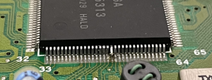
This method effectively disconnects color output on composite video, which removes a source of interference in the RGB signals. To do this, simply locate the pin, heat the pin with a soldering iron, and use metal tweezers to lift the pin so it no longer makes contact with the motherboard or either neighboring pins.
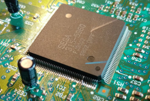
Location of the pin is dependent on what model VDP is on your board:
- Sega 315-5313 and 315-5313A: Pin 50 (15th down from the top-right corner).
- Sega 315-5487, 315-5660, 315-5700 and 315-5708: Pin 131
- Sega 315-5685 and 315-5786: Pin 103 (one down from the top-right corner of the chip, note that the top of the chip is facing the front of the console)
- Sega 315-5960: Pin 153 (8th up from the bottom-left corner).
After lifting the pin, test your console to ensure it is still functional. If it is not, inspect the neighboring pins to make sure you didn't accidentally lift them.
Subcarrier Bypass Board
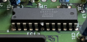
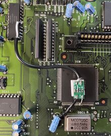
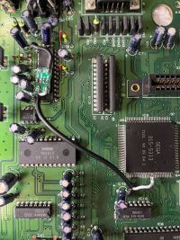
Created by Tianfeng, this board (download) sits between the lifted subcarrier pin on the VDP and the Sony CXA1145P chip. This is a good option if you want cleaner RGB but still want to preserve color on the composite output.
- Using double sided tape or similar product, mount the bypass board somewhere. Suggested places include on top of the VDP or on top of the CXA as shown below.
- Lift the subcarrier pin on the VDP as described in the section above.
- On most model 1s, lift pin 6 on the Sony CXA1145 encoder. On the model 2, remove capacitor C24 (C22 on the VA4 model 2). This will effectively isolate pin 6 of the encoder.
- Solder a shielded wire from pin 6 of the encoder (or the right pad of the removed capacitor on model 2s) to the
Pin6pad on the bypass board. Solder the shielding of the wire to pin 1 of the encoder and to the GND pin on the bypass board closest to the Pin6 pad. - Solder a wire from the lifted VDP pin to the
X-inpad on the bypass board. - Solder a wire from the GND pad near the
X-inpad to a ground the point. The negative leg of a nearby capacitor is suitable.
Subcarrier Ground Switch
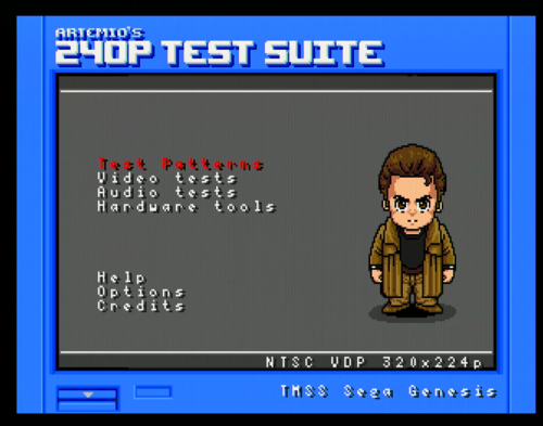
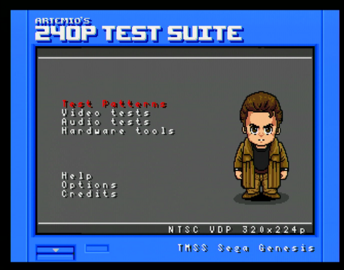
Grounding the subcarrier basically achieves the same thing as lifting the pin, and putting a switch in the ground wire can allow you to turn on/off the subcarrier signal. This lets you get the benefits of the subcarrier pin lift without lifting the pin and while preserving the ability to output Composite video.
- Solder a long wire to the subcarrier pin. There are a couple ways to do this:
- Solder directly to the pin without lifting.
- Solder to a component / trace / via that is connected to the pin (such as C102 on a Model 1 VA 6.5, or R61 [or the via under the CPU that R61 is connected to] on a Model 2 VA0, etc.).
- Solder a wire to the subcarrier pin on the video encoder (usually pin 6, Check the schematics for your encoder).
- Solder the other end of that wire to a SPST switch.
- Solder a wire to the other side of the switch and solder that wire to ground.
- Mount the switch somewhere:
- Removing the RF modulator on Model 1s leaves a nice hole for a switch
- Drilling a hole next to the AV connector on model 2s is a decent solution
- Run the wires outside the case and let the switch dangle
- Test the switch, you should see the jailbars reduced (and composite will have no color) when the switch is on/when the subcarrier is grounded.
Triple Bypass
This mod effectively moves the audio and video circuitry off of the motherboard, providing much cleaner RGB signals. More information and installation guides can be found on the Genesis:Triple_Bypass Mod page. Note that this will not completely remove jailbars caused by subcarrier interference, particularly for the model 2 VA2 and VA4 board revisions.
