Genesis:Triple Bypass Mod Model 2 VA0: Difference between revisions
m (Derf moved page Genesis:Triple Bypass Mod Model 2 va0 Install Tutorial to Genesis:Triple Bypass Mod Model 2 VA0 without leaving a redirect) |
No edit summary |
||
| (4 intermediate revisions by 3 users not shown) | |||
| Line 1: | Line 1: | ||
This document will serve as clear step-by-step instructions for installing the 3BP on the Genesis Model 2, revision VA0. | |||
== Sega Genesis Model 2 - VA0 Triple Bypass Install Tutorial == | == Sega Genesis Model 2 - VA0 Triple Bypass Install Tutorial == | ||
=== Introduction === | === Introduction === | ||
| Line 59: | Line 61: | ||
# Lift the RGB pins on the video encoder. These are pins 21, 22, and 23. Head the pin with your soldering iron then, using a narrow tool, lift the pin away from the pad. Make sure there is no solder linking the pin to the pad. | # Lift the RGB pins on the video encoder. These are pins 21, 22, and 23. Head the pin with your soldering iron then, using a narrow tool, lift the pin away from the pad. Make sure there is no solder linking the pin to the pad. | ||
# Remove resistors R62, R63, and R64. These are the RGB lines coming from IC6 to the video encoder. Removing these 3 resistors effectively cuts all current from reaching the video encoder along the RGB lines. | # Remove resistors R62, R63, and R64. These are the RGB lines coming from IC6 to the video encoder. Removing these 3 resistors effectively cuts all current from reaching the video encoder along the RGB lines. | ||
'''IMPORTANT''' - DO NOT REMOVE R50, R51, AND R52. These are required to remain IN CIRCUIT. Otherwise you'd have to install 3 x 5.6k resistors independently. Some guides and installers recommend removing the entire RGB circuit, but this is not entirely necessary. Lifting pins 21, 22, and 23 on the encoder AND removing R62, R63, and R64 along the RGB traces effectively disables the built-in RGB circuit. Leaving R50, R51, and R52 (the oem 3 x 5.6k resistors) in-place eliminates the needs for adding the 3 x 5.6k resistors as advised by RetroRGB and others. For more information on the 5.6k resistor "fix", check out this page: [https://www.retrorgb.com/fix-for-all-rgb-bypassed-sega-genesis.html Fix for all RGB bypassed Sega Genesis] | |||
'''Box 4'''<br /> | '''Box 4'''<br /> | ||
| Line 67: | Line 70: | ||
[[File:Md2va0 mainboad bottom large 1-2-3.jpg|thumb|Part 2 - Prepping the bottom side of the VA0 board]] | [[File:Md2va0 mainboad bottom large 1-2-3.jpg|thumb|Part 2 - Prepping the bottom side of the VA0 board]] | ||
'''(Reference the overview image and corresponding numbered boxes for the next few sections)'''<br /> | '''(Reference the overview image and corresponding numbered boxes for the next few sections)'''<br /> | ||
Phew! That wasn’t so bad, was it? Now let’s prep the bottom of the board. In this section we will tin each of the mount points for the 3BP input wires (box 1) and the 3BP board itself (box 2). | Phew! That wasn’t so bad, was it? Now let’s prep the bottom of the board. In this section we will tin each of the mount points for the 3BP input wires (box 1) and the 3BP board itself (box 2). Box 3 is left over from an older version of this guide and will not be used. | ||
<br clear=all> | <br clear=all> | ||
| Line 87: | Line 90: | ||
# Once trimmed, add a small amount of solder back to the flush pins to re-secure it to the board. | # Once trimmed, add a small amount of solder back to the flush pins to re-secure it to the board. | ||
# Reflow / add solder to the 2 pins circled in BLUE. These often crack over time on these models and will require reflowing or re-soldering. Do this now since you’re already here. | # Reflow / add solder to the 2 pins circled in BLUE. These often crack over time on these models and will require reflowing or re-soldering. Do this now since you’re already here. | ||
<br clear=all> | <br clear=all> | ||
== Part 3 - Prepping the Triple Bypass board == | == Part 3 - Prepping the Triple Bypass board == | ||
[[File:3BP board VA0 jumper settings.jpg|thumb|Part 3 - Prepping the Triple Bypass board]] | [[File:3BP board VA0 jumper settings.jpg|thumb|Part 3 - Prepping the Triple Bypass board]] | ||
This section involves getting the 3BP board ready. We need to solder a few jumper settings to make the board work with our Genesis revision. If you look on the back of the 3BP, you’ll see the jumpers we need to set under the line that reads, “M1va7 & M2va0-1.8”. Looking here, you’ll see that jumpers 2, C, D-Right, and E need to be bridged. | This section involves getting the 3BP board ready. We need to solder a few jumper settings to make the board work with our Genesis revision. If you look on the back of the 3BP, you’ll see the jumpers we need to set under the line that reads, “M1va7 & M2va0-1.8”. Looking here, you’ll see that jumpers 2, C, D-Right, and E need to be bridged. See the image on the left (before) for the exact points to bridge. | ||
'''Note: The instruction to solder D-right assumes that R21 is not present on the mainboard. If it is present, leave the D jumper unconnected''' (This is an artifact of the original Mega Amp instructions telling you to remove it). | |||
After bridging the required jumpers, tin all the inputs on the bottom and right edges of the 3BP board: YR, CR, XR, PSG, XL, CL, YL, 5V, S (CSYNC), R, G, B. | After bridging the required jumpers, tin all the inputs on the bottom and right edges of the 3BP board: YR, CR, XR, PSG, XL, CL, YL, 5V, S (CSYNC), R, G, B. | ||
Latest revision as of 00:25, 1 December 2022
This document will serve as clear step-by-step instructions for installing the 3BP on the Genesis Model 2, revision VA0.
Sega Genesis Model 2 - VA0 Triple Bypass Install Tutorial
Introduction
Installing the Triple Bypass Version 2 mod on your Genesis is easily one of the most beneficial things you can do for your gaming experience. Unfortunately information on installing the 3BP mod on the various revisions is scattered. This document will serve as a clear and step-by-step instruction on installing the 3BP on the Genesis Model 2, revision VA0. Revisions 1.0 and 1.8 are extremely identical to the VA0 and may benefit from this guide as well.
Models Supported
The following models are 100% supported by this guide.
- Model 2 - VA0
The following models are very similar in layout and may benefit extensively from this guide. It is your responsibility to verify if your model is compatible with this guide.
- Model 2 - VA1
- Model 2 - VA1.8
WARNINGS
Please read the below warnings before proceeding!
- This guide expects you to have a basic understanding of how to open up your Genesis Model 2 and to have basic soldering skills.
- This mod permanently alters your device.
- This mod should not be done by a beginner and is considered intermediate/advanced.
- Make sure power is disconnected before proceeding.
- After performing this mod you will no longer be able to use composite. You’ll be required to use component cables from this point forward.
- Proceed at your own risk!
Tools required:
- Flush cutters
- Snips
- Soldering iron
- Solder
- Flux
- Solder wick
- 28 or 30 awg wire
Start by removing the shell from your console. Remove the 4 screws at the bottom then turn it back upright and lift off the top shell. Remove the screws on the metal shielding and lift the shield off. Next, remove the 2 screws on the sides of the cartridge slot. Now you can lift the motherboard out of the bottom half of the shell.
Part 1 - Prepping the top side of the VA0 board
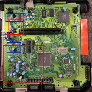
(Reference the overview image and corresponding numbered boxes for the next few sections)
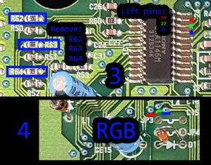
The “scariest” part of this mod is certainly the removal of the many components on the board. Don’t fret… It’s not as bad as it sounds! Use the many diagrams throughout this guide as a reference for each step. Each part below will have one or more images, and some sub-sections will have "boxes". These boxes are for zoomed-in regions on the motherboard to show more detailed instructions. For example: Lifting the RGB pins will be in box 3. Be sure to read the captions under each image to correctly identify which Part and which Box the image belongs to.
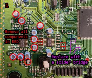
Box 1
- Remove all the items that are circled or boxed in RED. You can use your flush cutters to ship off the capacitors, then use your solder wick to remove the remaining solder and pull out the remaining pins from the snipped capacitor.
- Replace the items in PURPLE with solder bridges.
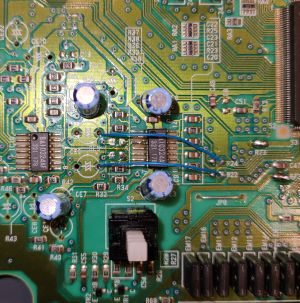
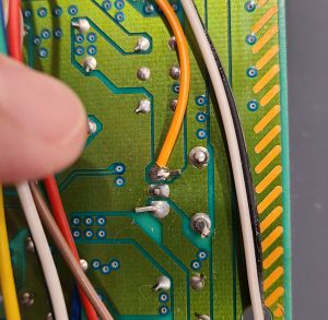
There's one more thing to do in this area after you remove all components and created the solder bridges. You need to connect the right side of R24 and the right side of R22 to the POSITIVE (+) through holes for CE5 and CE2. Once the wire is pushed through, you can apply some solder on the bottom side of the board (See part 2, box 1 in the next section for details).
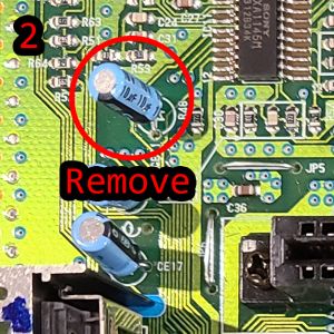
Box 2
- Remove the single capacitor circled in RED.
Box 3 & 4
Box 3
- Lift the RGB pins on the video encoder. These are pins 21, 22, and 23. Head the pin with your soldering iron then, using a narrow tool, lift the pin away from the pad. Make sure there is no solder linking the pin to the pad.
- Remove resistors R62, R63, and R64. These are the RGB lines coming from IC6 to the video encoder. Removing these 3 resistors effectively cuts all current from reaching the video encoder along the RGB lines.
IMPORTANT - DO NOT REMOVE R50, R51, AND R52. These are required to remain IN CIRCUIT. Otherwise you'd have to install 3 x 5.6k resistors independently. Some guides and installers recommend removing the entire RGB circuit, but this is not entirely necessary. Lifting pins 21, 22, and 23 on the encoder AND removing R62, R63, and R64 along the RGB traces effectively disables the built-in RGB circuit. Leaving R50, R51, and R52 (the oem 3 x 5.6k resistors) in-place eliminates the needs for adding the 3 x 5.6k resistors as advised by RetroRGB and others. For more information on the 5.6k resistor "fix", check out this page: Fix for all RGB bypassed Sega Genesis
Box 4
Now we need to identify the RGB vias that we’ll use to connect the 3BP. These 3 vias are located on the RGB lines. The easiest way to find them is to look at the image to the right. On your board, they are located next to the label “L4”. You can also follow the traces from R62, R63, and R64 towards the front of the board. There will be 3 vias that go to the bottom of the board, then over an inch or so, then back up to the top of the board. From this point, they run over to IC6.
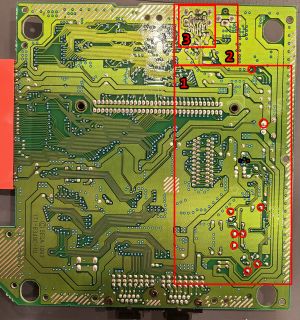
Part 2 - Prepping the bottom side of the VA0 board
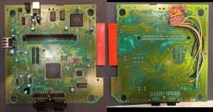
(Reference the overview image and corresponding numbered boxes for the next few sections)
Phew! That wasn’t so bad, was it? Now let’s prep the bottom of the board. In this section we will tin each of the mount points for the 3BP input wires (box 1) and the 3BP board itself (box 2). Box 3 is left over from an older version of this guide and will not be used.
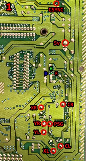
Box 1
- Tin each of the through holes circled in RED (that used to be capacitors) with a small bit of solder.
- Add additional solder to the 5V pin
- Scrape the solder mask off from the CSYNC via to expose the shiny copper. Be careful not to scrape too hard or too much as you don’t want to damage the copper. Tin with a small bit of solder.
- Scrape the solder mask off of the 3 RGB vias to expose the shiny copper. Be careful not to scrape too hard or too much as you don’t want to damage the copper. Tin with a small bit of solder.
WARNING: DO NOT CUT OR DAMAGE THE RGB TRACES ANYWHERE FROM IC6 TO R50, R51, AND R52. It’s important to keep these resistors in circuit.
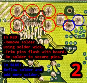
Box 2
- The pins circled in RED at the DIN port are currently too large for the 3BP board to sit flush with the motherboard. We need to trim them down. We also need to secure the pins for the power port.
- Using solder wick, remove the solder from each of the pins circled in RED. Then, using flush cutters, trim the pins flush to the board.
- Once trimmed, add a small amount of solder back to the flush pins to re-secure it to the board.
- Reflow / add solder to the 2 pins circled in BLUE. These often crack over time on these models and will require reflowing or re-soldering. Do this now since you’re already here.
Part 3 - Prepping the Triple Bypass board
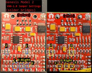
This section involves getting the 3BP board ready. We need to solder a few jumper settings to make the board work with our Genesis revision. If you look on the back of the 3BP, you’ll see the jumpers we need to set under the line that reads, “M1va7 & M2va0-1.8”. Looking here, you’ll see that jumpers 2, C, D-Right, and E need to be bridged. See the image on the left (before) for the exact points to bridge.
Note: The instruction to solder D-right assumes that R21 is not present on the mainboard. If it is present, leave the D jumper unconnected (This is an artifact of the original Mega Amp instructions telling you to remove it).
After bridging the required jumpers, tin all the inputs on the bottom and right edges of the 3BP board: YR, CR, XR, PSG, XL, CL, YL, 5V, S (CSYNC), R, G, B.
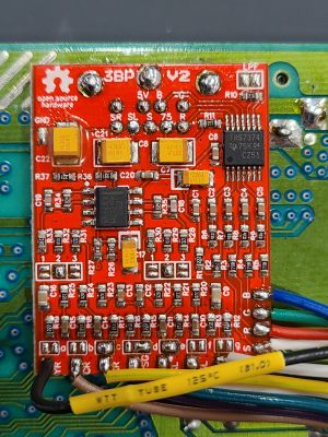
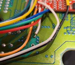
After tinning the inputs, line up the output through holes (at the top of the board) with the DIN pins. The 3 large holes line up with the 3 upper most pins of the DIN. The rest of the holes line up accordingly. There’s only one way the 3BP will sit on the DIN, so make sure it lines up and sits nicely. Once it’s set, start by soldering the 3 large holes to secure it into position. Then add a generous amount of flux to the smaller holes. Solder each of these output holes with just enough solder to make contact with the pin beneath it. Be careful not to use too much solder because you don’t want to bridge two adjacent holes. Use a multimeter to make sure there is no continuity between any two adjacent holes.
Part 4 - Solder all connections
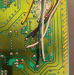
Now it’s time to connect each of the 3BP inputs to their corresponding sources on the board. Using Box 1, solder each corresponding 3BP input to its motherboard source. For example: Solder YR on the 3BP to the source labeled YR on the bottom of the board. CR to CR. PSG to PSG. When routing the wires, make sure to be clear of the slot pins. When the board is put back in the shell, there's a small plastic bracket that sits under the slot. If you aren't careful to route your wires away from the slot, you won't be able to reassemble the console. Use Box 1 as a reference for each solder point.
Part 5 - Bottom shield plate modification
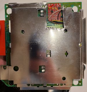
Even with the 3BP sitting flush against the motherboard, it’s still too thick to fit with the metal shield in place. You can remove the metal shield if you wish, but this is not recommended as it leaves the rest of the motherboard exposed to static and dust from the floor. Simply use snips to trim the shield enough to clear the 3BP board.
Conclusion
Finally, reassemble the console. If you followed the instructions exactly you should now have a successfully bypassed Genesis Model 2 va0. Plug in component to your display and enjoy!
