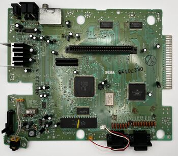
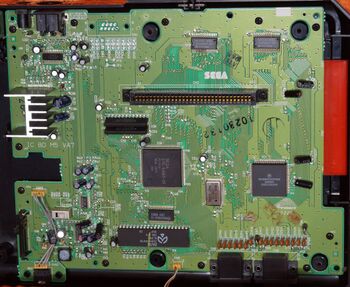
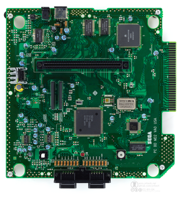
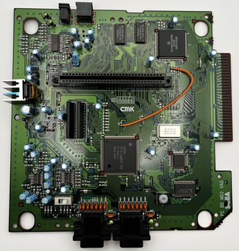
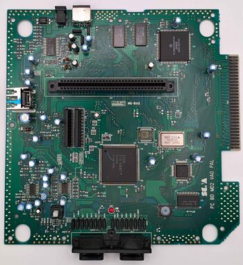
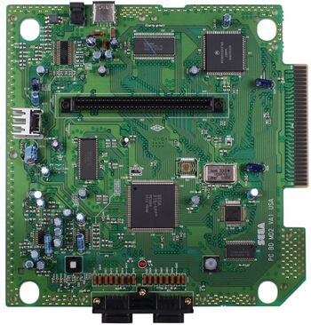
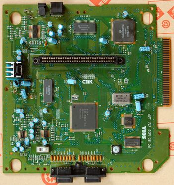
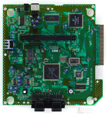
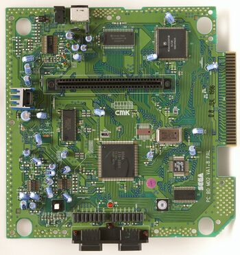
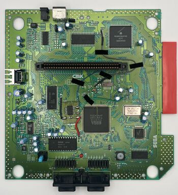
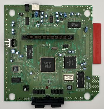
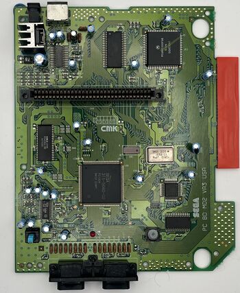
Genesis:Motherboard Differences
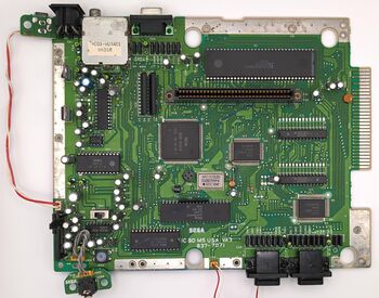
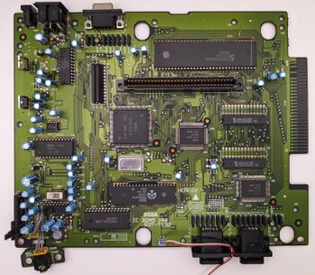
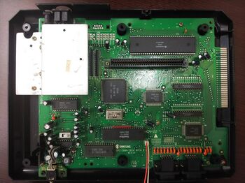
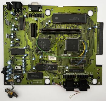
There were numerous motherboard revisions of the standalone Genesis and Mega Drive consoles. This page serves to document these board revisions and the technical information for each.
Model 1
837-6656 - "VA0" (1988, Japan)
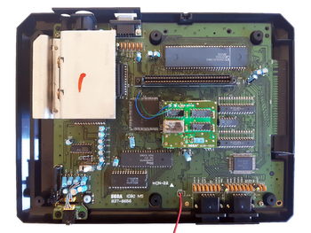
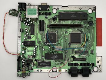
This is the earliest revision of the model 1 and is only found in Japanese Mega Drive consoles. These contain a small daughterboard (part number 839-0231) which has the master oscillator crystal, a 74LS74 D-type flip flop and two 74161 (one 74LS161 and one 74F161) 4-bit counter chips. During manufacturing, Sega discovered that the EDCLK (external dot clock) signal did not work properly in the H40 video mode. Using the master clock frequency and the horizontal sync (HSYNC) signal, the daughterboard generates a proper EDCLK signal which is fed back into the board. Sega also included a discrete 74LS00 logic gate on the motherboard to fix RAM compatibility issues with Master System games.[1]
Although the board is not designated as such, it is commonly referred to as the "VA0" in keeping with Sega's revision naming practices and the fact that it was the first board revision produced.
On the VA0, the preamp is slightly overdriven, resulting in audio distortion in certain games. This can be changed by substituting several capacitor and resistor values on the underside of the motherboard. Video quality is also compromised as composite video exhibits "rainbow banding" and the RGB output has noticeable jailbars. These would be carried over into later model 1 revisions.
Sega only produced the VA0 for a fairly short period, as it was quickly replaced by the VA1 (detailed below) in order to cut production costs and presumably to reduce the amount of manual labor involved during assembly, since the daughterboard and its connecting wires had to be soldered in by hand.
VA1 (1989, Japan)
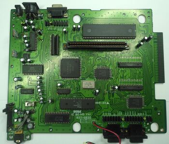
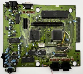
Introduced very early in 1989, the VA1 incorporated the EDCLK daughterboard and discrete 74LS00 logic gate into an additional gate array chip, the 315-5339. Like the "VA0" before it, this board is only found in Japanese Mega Drives. It also has the same issue with the overdriven preamp over the headphone output.
VA2 (1989, Japan and North America)
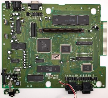
This is the first board revision for the Genesis and is also found in Japanese Mega Drive consoles. On this revision, the 315-5339 EDCLK generator chip was replaced with the 315-5345, which added an additional bus acknowledgment signal (/BGACK) going to the VDP. It uses this signal to prevent potential glitches related to DMA (direct memory access) refresh timing.[2] In particular, the Japanese-only release Osomatsu-kun Hachamecha Gekijou does not initialize the system memory at startup [3], a glitch which is addressed by the 315-5345.
No other major changes were made.
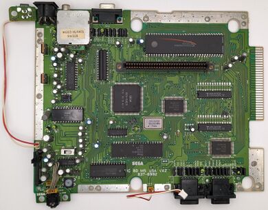
Sega made some changes to the board layout for North American models in order to accommodate an internal RF modulator and RF shielding, neither of which the Japanese Mega Drive ever had. The retention of the EXT port also meant that the power input jack had to be moved onto a separate PCB, connected to the motherboard by two wires. These layout differences between Japanese and Western consoles would be carried on into all later model 1 revisions until the VA7.
VA3 (1989-1991, Brazil and North America)
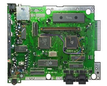
Introduced in late 1989, the VA3 revision was only used in North American and Brazilian consoles (being the first revision for the latter). The 315-5308 bus arbiter and 315-5345 EDCLK generator were consolidated into a single IC, the 315-5364, likely to reduce production cost. A 4.7k ohm pull-up resistor array was also added on the Z80's data bus pins, though it was soldered directly onto the Z80 itself and not placed on the board. The audio circuitry was changed as the overdriven preamp from previous revisions was fixed and some additional low-pass filtering was added to the output stage, which slightly muffled the audio. Despite this, the audio quality from the VA3 is generally held in high regard by enthusiasts, and this variant is often used as a baseline for audio quality in Genesis consoles. Future model 1 revisions up to the VA7 would use this audio circuit. Its audio profile is also the basis for the audio portion of the Triple Bypass modification board.
Most VA3s manufactured in Japan have carbon coated pins on the expansion port and bare copper on the ground plane instead of having HASL plating on both. These also have Rubycon capacitors which are higher quality than the Chhsi capacitors typically fitted on consoles manufactured in Taiwan. Japanese-built VA3 consoles will have a serial number starting with "90S" or "B10"[4].
For Brazilian VA3s, some changes were made in order for them to output PAL-M video. A 53.634 MHz master oscillator was fitted and pin 7 of the video encoder was directly connected to GND to force it into PAL mode; this pin is normally controlled by JP3 and JP4, which also set the VDP's video frequency.[5]
VA4 (1989-1992, Asia, Japan, Korea and PAL)
The VA4 is largely identical to the VA3, and was first introduced in late 1989 in Japanese Mega Drive consoles. It was also the first board revision for Asian, PAL and Korean consoles. The video encoder was flipped around with the front of the chip pointing towards the front of the console. In addition, the resistor array on the Z80's data bus was given a footprint on the board and was not soldered directly onto the Z80 as before. These are the only significant differences between the VA3 and VA4. Composite video output was slightly changed with the reduction of the "rainbow banding" common on earlier revisions, though it is still present to some degree.
Asian and PAL VA4 boards, which were introduced in late 1990, follow the same board layout as North American board revisions and also have an internal RF modulator. PAL VA4 boards made in 1992 (such as the one pictured above) use a die-shrunk[6] version of the VDP, the 315-5313A (Yamaha FC1001).
SPC-200/201R Rev. A (1992-1993, Korea)
By 1992, Samsung began manufacturing their own motherboards for the Super Gam-Boy/Super Aladdin Boy, which was the version of the Mega Drive sold in Korea. This board is heavily based on the VA4 and uses the same layout, but does not have the EXT port populated.
VA5 (1990-1991, Japan)
Introduced in late 1990, this board design saw further consolidation by combining the 315-5309 I/O chip and 315-5364 bus arbiter into a single ASIC, the 315-5402. This particular board revision was only used in Japanese Mega Drives. The region and video frequency jumpers were relocated from the lower center to a new position closer to the expansion port.
One interesting quirk with this board revision is the presence of three jumper wires which are sometimes mistaken as an aftermarket modification.[7] These jumper wires connect the CE (Chip Enable) and OE (Output Enable) signals of the two 68000 RAM chips to the main system bus; JP5 connects the CE signal of both chips, JP6 the OE signal of IC2, and JP7 the OE signal of IC3. It is unknown why these signals were connected using jumper wires and not properly routed on the board itself as on previous revisions. The jumper wires are also present on the VA6 and its variants (detailed below).
Two different versions of the 315-5402 I/O chip exist, one which completely lacks TMSS, and another which will display the TMSS screen only if the system's region setting is changed from Japanese to English/export[8], which is accomplished by cutting the trace on jumper JP1 and connecting JP2 in its place.
This was the last board revision where Sega used 68000 CPUs made by Signetics, who had been Sega's sole supplier of this component for the Mega Drive since its launch. During 1991, Sega began sourcing CPUs from Motorola and Hitachi instead, and VA5s manufactured in 1991 (denoted with a "1" as the second digit of the serial number) have Motorola CPUs.
VA6 (1991-1992, Asia, Brazil, Japan, North America and PAL)
Completely identical to the VA5 but substitutes the I/O chip with the 315-5433, which adds the TradeMark Security System (TMSS) lockout screen ("Produced by or Under License by Sega Enterprises, Ltd") that appears for several seconds before playing any game. TMSS checks for the word "SEGA" at two locations in the game code, and if it is not at either one of these memory locations, the game will not run. TMSS would be present in all Genesis/Mega Drive consoles from this point forward.
In addition, the VA6 was the last board revision in most markets to have the EXT port. Sega had planned to release a modem which used this port, but it ultimately only saw a Japanese release (known there as the Mega Modem), and Sega abandoned their plans to release it elsewhere.
The VA6 first appeared in US Genesis consoles that were sold beginning in September 1991[9], with other regions following later that year. VA6 boards found in later Japanese Mega Drives used the revised 315-5313A VDP. In PAL regions, the VA6 is extremely uncommon and only appeared in certain Mega Drives produced in Japan during 1992 with a serial number starting with "A"[10] or "Q"[11].
VA6.5 (1992-1993, Asia, North America and PAL)
The VA6.5 is simply a VA6 with the EXT port and its line filters removed, since the EXT port was unused in most markets. No other changes were made, though consoles with this board have a large blank space on the rear where the EXT port once was. The "VA6.5" name originates from Sega service documentation[12] and is not denoted on the board itself. Many of these used the 315-5313A or 315-5313A-01 VDP.
VA6.8 (1993, PAL)
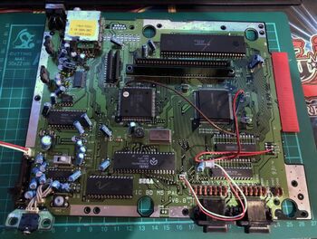
The VA6.8 revision is largely identical to the VA6.5 but has a surface-mount Fujitsu MB3514 video encoder in place of the DIP Sony CXA1145P found in all other models. No other changes were made.
Due to erroneous information online, the VA6.5 is commonly confused for this revision. Several[13][14][15][16] places online will sometimes refer to the existence of a US VA6.8, but they are actually referring to the VA6.5. Actual VA6.8s were only produced for PAL regions and appear in no other consoles. This was the final board revision for the PAL model 1.
VA7 (1992-1993, Brazil, Japan, North America and Taiwan)
Introduced in mid-1992, the VA7 was the most drastic revision of the model 1 released. It is the first standalone Genesis/Mega Drive to use the Yamaha FC1004 ASIC found in most model 2 consoles, which combines the 315-5313 VDP, 315-5433 I/O controller, and a modified Yamaha YM3438 audio chip into a single chip. Specifically, the VA7 uses the 315-5487 variant, which first debuted in the Japan-only Wondermega console earlier that year. All VA7s use a surface-mount version of the Sony CXA1145 encoder, a PLCC version of the Motorola 68000 CPU, and only have a single 7805 voltage regulator as opposed to two like on previous board revisions. Both the main RAM and Z80 RAM were also changed to SOP type surface mount chips. These changes also allowed for all of the SMD passive components (resistors, capacitors, etc.) to be moved to the top side of the board.
On non-Japanese consoles, the ports on the back have been shifted significantly towards the center, having the AV out occupy where the EXT port used to be (except on Japanese VA7s, which still have the EXT port present), which leaves a large gap to the right. This was also the first Western revision to have the power jack on the motherboard itself, as the revamped board layout allowed for having both the RF modulator and power jack on the same PCB. VA7s sold in Taiwan use the same board layout as the Japanese VA7, but the EXT port and its line filters are unpopulated, leaving a large blank spot on the rear panel similar to the VA6.5.[17] Taiwan seems to have been the only Asian country outside of Japan where the VA7 was sold.
The audio fidelity was noticeably changed compared to all previous model 1 revisions, making it less desirable as a result. This is due to Sega using an inadequate amplifier circuit and can be corrected using a modification board such as the Triple Bypass or Mega Amp. Some of the components in the audio circuitry can also be swapped with different ones to alter the audio quality without these boards. Despite this, video quality is slightly cleaner than previous revisions, with only some minor jailbars on the blue output and the near elimination of the "rainbow banding" on composite.
Although it is possible to region mod these as with any other Genesis/Mega Drive console, switching a VA7 to 50 Hz mode will cause all audio to stop working for many games, and some games will even crash. This is likely due to the use of the original 315-5487 ASIC, which was only used in NTSC consoles and has a broken 50 Hz mode. Later versions of this ASIC such as the 315-5660 fixed this problem, but by that time, Sega had discontinued the model 1 in favor of the cost-reduced model 2.
Model 2
VA0 (1993, All Regions)
The first board revision for the model 2, a smaller and greatly cost-reduced redesign of the Genesis/Mega Drive. It is very similar to the VA7 model 1 with many of the same components, though the Z80 CPU was changed to a much smaller QFP (quad flat pack) package in order to save space.
Early NTSC boards made use of the 315-5487 ASIC from the VA7, which has a broken 50 Hz mode and so this particular chip was not used in the PAL Mega Drive II. In very early PAL VA0s, Sega used the 315-5487• (dot after the designation), a version of this ASIC which had a fixed 50 Hz mode. Sega would switch out both ASICs with the 315-5660 early in the model 2's life, and this is found in the vast majority of these consoles. The 315-5708 variant was also used, which was a Fujitsu-manufactured version of the 5660. For some unknown reason, Japanese and Asian Mega Drive 2 consoles use a slide switch for power like the model 1 instead of a push button switch, and lack a power LED.
In terms of sound quality, the VA0 is similar to the VA7, though the PSG volume is reduced and so does not distort as much. The FM output is still very distorted and has some hissing.
RGB output is also similar to the VA7, again with only some minor jailbars on the blue output. However, composite video can differ based on what video encoder is used. Most North American consoles with this revision used the Samsung KA2195D, which has fairly blurry video output with noticeable jailbars. Most Japanese and some North American systems used the Sony CXA1145M, which was previously used in the VA7 and has less artifacts than the KA2195D. All PAL Mega Drive IIs with this revision and the later VA1 and 1.8 boards had the Fujitsu MB3514 encoder, which is similar in output to the CXA1145. A few Japanese Mega Drive 2s also used this particular encoder.
All VA0s come with or without HAL (Hot-Air Solder Leveling), although the "HAL" text is not always present on the boards which have it. In addition, it was also manufactured with or without plated through-holes, and the layout is slightly different between these variations. The non-plated variations have extra vias and also have jumper links in place of some power traces.
This and the following two board revisions are among the most difficult to region mod as the two pins on the ASIC responsible for region and video frequency are hardwired to either 5V or GND depending on the console's region. Region modding one of these will involve either very careful trace cutting or lifting these delicate ASIC pins.
Early Brazilian Mega Drive III consoles have a VA0 board but with a small RF modulator board crudely soldered onto the side of the board, with the RF output jack sticking out of the side of the console. In later versions, TecToy used a board revision of their own design, which was heavily based on the VA1/VA1.8. This revision integrated the RF out on the motherboard (with the output jack now at the rear) and featured an internal power supply with switchable input voltage.
VA1 (1993-1994, All Regions)
The VA1 differs from the VA0 mainly in that it consolidates the two VRAM chips and two 68K RAM chips with one chip each - and there are major trace routing changes to accommodate this. Some resistor values were also changed in the audio circuit in an attempt to reduce distortion: R42 through R45 were increased from 4.7k ohm to 7.5k ohm, while R81 was decreased from 6.8k to 4.7k. Like the VA0, some VA1s had plated through-holes while others did not. Video encoders were also the same as before.
This was also the final board revision for Japan.
VA1.8 (1994-1996, Asia, North America and PAL regions)
It is unclear what exactly is different between the VA1 and VA1.8, as the boards appear mostly identical with the exact same components and no documentation of this difference has been found. Some VA1.8 boards have two wires between the positive and negative pins of the power jack and two solder pads on the underside which are not present on earlier boards. In addition, some US VA1.8s had the Fujitsu MB3514 video encoder, making them the only standalone US Genesis consoles to use this particular encoder. Sega did not use any Sony encoders on the 1.8.
VA2 (1994, North America)
Introduced during 1994, the VA2 is the first of two model 2 revisions which use a discrete YM2612 FM chip like most model 1s, as the Toshiba-manufactured ASIC (Sega 315-5786) used in this model does not have a YM3438 core. Sound-wise, the VA2 is very different than previous revisions; the volume balance was altered with the FM channels being considerably louder than the PSG and external audio from both the cartridge and expansion ports. Sega used the 315-5684 audio amplifier chip as opposed to the dual LM324-based setup used in previous model 2 revisions. Some consoles make use of the Samsung KA2195D video encoder while others have the Sony CXA1645, an improved version of the CXA1145 used in previous consoles. Largely due to the board layout, the RGB output has very noticeable jailbars which cannot be totally eliminated by a Triple Bypass mod. The only way to eliminate these jailbars is to lift pin 103 of the ASIC from the board and either leave it disconnected (which will disable color over composite) or rewire it to the video encoder. More information on this can be found on this page.
The VA2 can also be identified by the presence of a small "bodge" PCB with a 74HC14 Schmitt trigger. This fixes an issue with the /ASEL signal on pin B26 of the cartridge port, used by Virtua Racing and the 32X. In addition, there is a shielded wire which routes the clock signal from the ASIC to the CPU, tacked down by either tape (VA2s made in China) or hot glue (VA2s made in Indonesia). These bodges are also visible with the cartridge flaps opened, making this easy to tell apart from other revisions.
Region modding one of these boards is as easy as a model 1, as Sega added jumper traces for both region and video frequency instead of directly wiring the corresponding ASIC pins to 5V. In this case however, the jumper traces are located on the underside of the board and not topside like most model 1 revisions.
This revision was only used in North American Genesis consoles.
VA2.3 (1995-1996, North America)
During 1995, Sega introduced a revised version of the VA2 known as the VA2.3. Much of the board layout was changed on this revision, with many major components being shuffled around and the Schmitt trigger circuit now being integrated into the board. As a result of the changed layout, the RGB output from this board is much cleaner than the VA2 and is similar to previous model 2 revisions. The different layout also eliminated the separate clock signal wire for the 68000 since it was positioned much closer to the main ASIC.
Sega used two different ASICs made by Toshiba in the VA2.3, the 315-5685 (TC6158AF) and 315-5786 (T9N13BF), with the older 5685 being used in later build VA2.3s. The 5685 has a flawed VDP core with a broken shadow and highlights mode and glitched raster effects. These issues were fixed in the 5786, which had been used in all VA2s and is found in earlier VA2.3s. More information regarding the issues on the 315-5685 can be found on this page.
VA2.3s manufactured in China (serial numbers beginning with "162" or "752") had the CXA1645 encoder while those manufactured in Malaysia (serial numbers beginning with "452") or Thailand (serial numbers beginning with "252") had the KA2195D.
As before, the VA2.3 is only found in North American Genesis consoles. Most VA2.3 consoles can be identified by their different model number, MK-1631A; consoles with this model number also have the 315-5685 chip.
VA3 (1994-1996, North America)
The first of the short board revisions. It uses a variant of the FC1004 ASIC as used in the VA0 through 1.8, but has a simplified audio section based on the 315-5684 amplifier chip instead of two separate LM324 op-amp chips. This in addition to some layout changes allowed Sega to reduce the size of the motherboard, cutting down production costs in the process. As with the VA0 through 1.8, some VA3s have plated through-holes while others do not.
Identifying these can be done by looking at the RF shielding through the bottom vents. If the shielding doesn't extend all the way across the width of the console, and does not have rectangular holes, it will be this revision. Sega used three different video encoders on the VA3, the CXA1145M, CXA1645 and the KA2195D. The encoder used can be roughly determined by the serial number; if it starts with "163", "253" or "463", it is almost guaranteed to have a Samsung encoder. Serials starting with "743", "753" or "R43" are extremely likely to have a Sony encoder, with the latter two being more likely to have a CXA1645. The audio fidelity was drastically changed, but the PSG volume is reduced compared to the VA0 through 1.8, and the overall frequency response is lower at higher frequencies.
Most VA3s use the 315-5660 ASIC, but a few made use of the 315-5700 (Yamaha FF1004) which was also used in the Nomad handheld. As with the VA0 through VA1.8 boards, the ASIC pins for selecting region and video frequency are hardwired to 5V. However, region modding a VA3 is somewhat easier as Sega added an exposed pad for each of these pins, meaning a simple trace cut is all that is needed to isolate these pins.
Like the VA2 and VA2.3 consoles, this board revision is only found in US Genesis consoles.
VA4 (1996-1998, Asia, Brazil, Korea, North America and PAL)
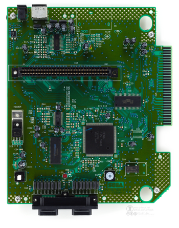
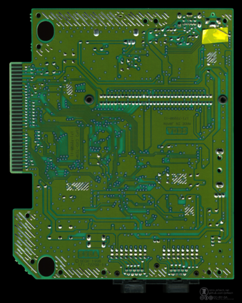
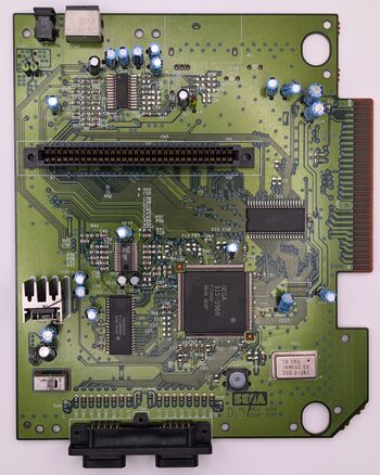
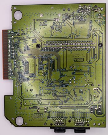
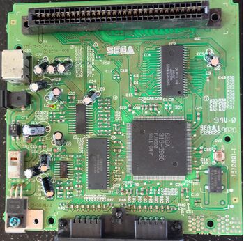
This was the final board revision for the model 2. It is especially notable in that it is the first Genesis console to use a GOAC (Genesis On A Chip) ASIC, specifically the Sega 315-5960 (Yamaha FJ3002). This incorporates all of the major components of the console (68000, Z80, VDP, YM3438, I/O controller, Z80 RAM) into a single chip, save for the main RAM, video RAM, video encoder and audio amplifier. Due to this change, the VA4 also consumes far less power than any other model 2. This is reflected by the position of the 7805 voltage regulator on North American and PAL units, where it is mounted horizontally on the motherboard and partially uses the top RF shield as a heat sink.
To identify one of these, look for two square cutouts on the shielding visible through the bottom vents. This was the only board revision in Asia, PAL regions and South Korea to use the 3/4 board size, making it even easier to identify in those regions. These will also have compatibility issues with both revisions of the 32X, which can be bypassed by loading 32X games from a flash cart instead of using original cartridges.
All US VA4s use the Sony CXA1645 encoder, which provides slightly improved composite video with less artifacts than its implementation on the VA3. The RGB output has some noticeable jailbars due to the routing of the color subcarrier trace. Like with the VA2, this can be fixed by either disconnecting or rerouting it away from the board. Some Asian and PAL VA4 boards instead feature a ROHM BH7236AF encoder, which is pin-compatible with the CXA1645. Curiously, Sega added the footprints for an internal RF modulator and its support circuitry, though no VA4 ever had these populated.
Both region and video frequency are set by 0 ohm jumpers for all VA4s. Region is selected by R31 (JP) or R32 (EN), and video frequency is controlled by R33 (50 Hz) or R34 (60 Hz).
Later VA4s in North America were sold under license by Majesco in 1998, who marketed the Genesis as a budget console. The build quality is largely identical to the earlier Sega-built examples, and these consoles are noted by their different model number (MK-1451) and a white model/serial number label.
Genesis 3
VA1 (1998)
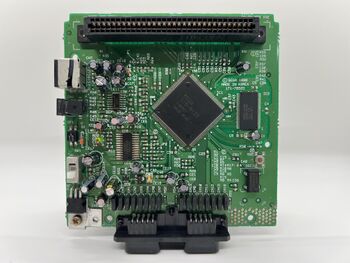
Essentially a highly condensed VA4 model 2 without an expansion port. Although it is not compatible with the 32X or Master System games, it can be modified for these due to it using the same 315-5960 GOAC as the VA4 model 2. One other major change is that stereo sound was omitted, and all audio goes through a single LM324 op-amp; external audio from the cartridge port was not passed through. The Sony CXA1645 video encoder was also carried over.
VA2 (1998-1999)
The VA2 uses a different GOAC, the 315-6123 (Yamaha FQ8002). This board also combined both the main RAM and video RAM into a single 128 KB SDRAM chip, leaving it, the video encoder (CXA1645) and audio amplifier (LM324) as the only remaining discrete ICs. 32X and Master System compatibility cannot be restored on this revision; only Game Genie and Virtua Racing compatibility issues are fixable on the VA2. The TAS instruction in the 68000 CPU was also fixed, which breaks compatibility with the game Gargoyles. The video and audio output quality were not changed.
References
- ↑ http://gendev.spritesmind.net/forum/viewtopic.php?t=2922
- ↑ https://twitter.com/nukeykt/status/1718625118031839563#m
- ↑ https://segaretro.org/Osomatsu-kun_Hachamecha_Gekijou/Bugs
- ↑ https://imgur.com/a/genesis-b10000996-z7Deeg2
- ↑ https://www.youtube.com/watch?v=NQeTLohYzTg
- ↑ https://github.com/emu-russia/SEGAChips/tree/main/VDP
- ↑ https://www.reddit.com/r/SEGAGENESIS/comments/sd1hhj/does_anyone_know_what_these_wires_are_i_found/
- ↑ https://gendev.spritesmind.net/forum/viewtopic.php?t=2191#p27395
- ↑ https://law.justia.com/cases/federal/district-courts/FSupp/785/1392/2144879/
- ↑ https://www.reddit.com/r/Megadrive/comments/1dwq0w6/super_rare_sega_mega_drive/
- ↑ https://www.youtube.com/watch?v=Bq2daWfC-SA
- ↑ https://consolemods.org/wiki/images/6/6b/PAL_Mega_Drive_Model_1_Service_Manual.pdf
- ↑ https://forums.atariage.com/topic/246707-new-genesis-va65-vs-va68/
- ↑ http://nerdlypleasures.blogspot.com/2017/01/sega-genesis-is-stinker-really-that-bad.html
- ↑ https://www.sega-16forums.com/forum/console-talk/genesis-does/22695-sega-genesis-mega-drive-manufacture-date-registry?p=920661#post920661
- ↑ https://web.archive.org/web/20230428012857/https://www.sega-16.com/forum/showthread.php?7796-GUIDE-Telling-apart-good-Genesis-1s-and-Genesis-2s-from-bad-ones
- ↑ https://169.45.167.69/forum/showthread.php?31762-NTSC-Asia-Mega-Drive
