File:Phat RGH3 Diagram 2.jpg: Difference between revisions
Jump to navigation
Jump to search
(This was intended overrite the old diagram, but it was a different format so now it is a seperate picture. It is a diagram showing optimal solder points and wire routing for RGH 3 on Falcon/Jasper/Tonasket motherboards.) |
(No difference)
|
Latest revision as of 08:29, 1 May 2024
Summary
This was intended overrite the old diagram, but it was a different format so now it is a seperate picture.
It is a diagram showing optimal solder points and wire routing for RGH 3 on Falcon/Jasper/Tonasket motherboards.
Licensing
This file has been released into the public domain by the copyright holder, its copyright has expired, or it is ineligible for copyright. This applies worldwide.
- Specify a reason as to why it is in the public domain and any limitations that should be noted.
- Specify the author who released it into the public domain.
File history
Click on a date/time to view the file as it appeared at that time.
| Date/Time | Thumbnail | Dimensions | User | Comment | |
|---|---|---|---|---|---|
| current | 08:29, 1 May 2024 | 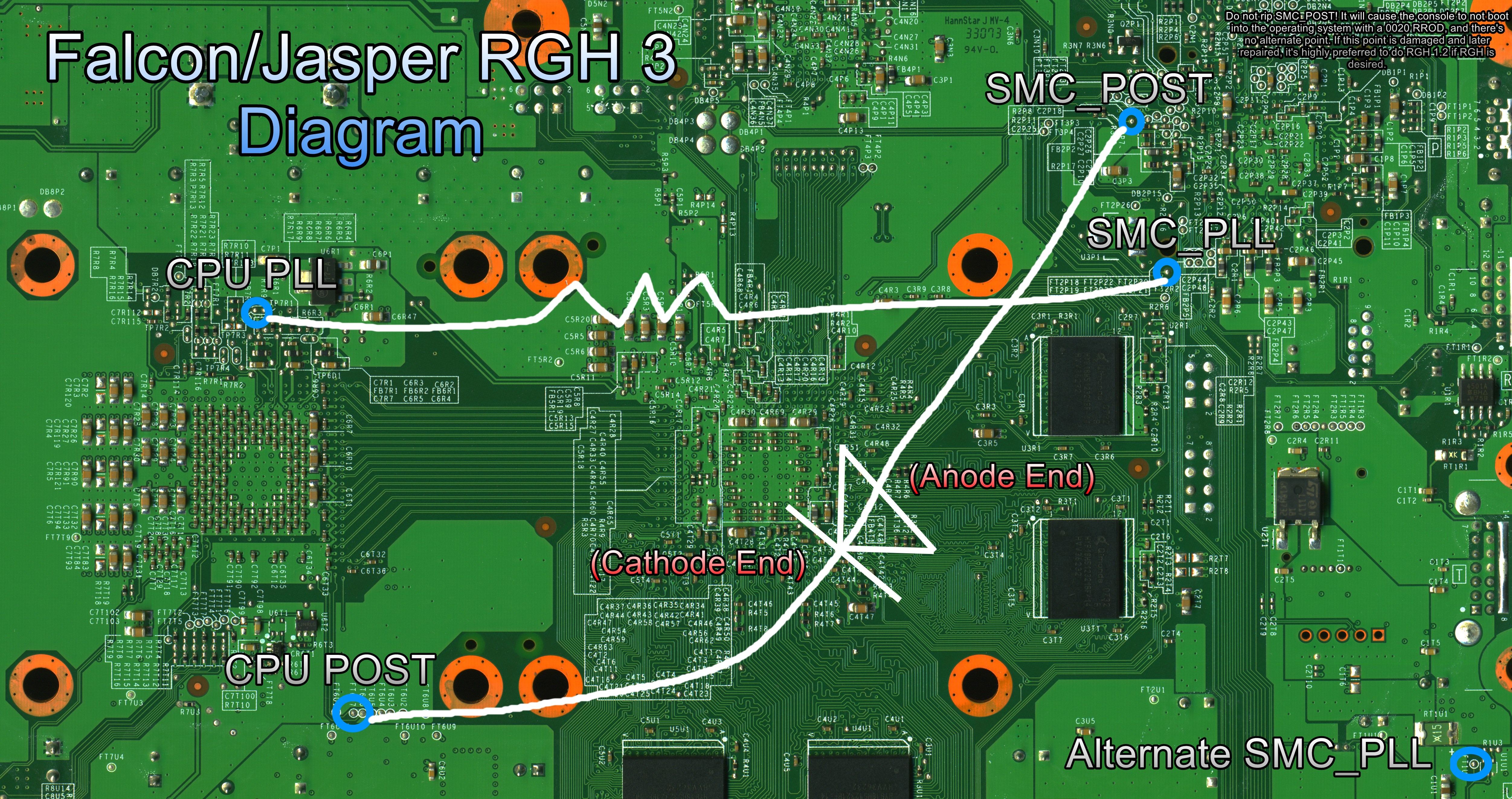 | 5,006 × 2,644 (3.36 MB) | Nadaman (talk | contribs) | This was intended overrite the old diagram, but it was a different format so now it is a seperate picture. It is a diagram showing optimal solder points and wire routing for RGH 3 on Falcon/Jasper/Tonasket motherboards. |
You cannot overwrite this file.
File usage
The following page uses this file: