Master System:Convert PAL System to NTSC
While the Sega Master System achieved little success in North America, it saw much better luck in PAL regions, especially in Europe and Australia. Because of this, Master System consoles, especially the smaller Master System II, are considerably more plentiful in those regions than in North America. In recent times, it can actually be less expensive to buy a PAL system online than a comparable NTSC system. However, PAL SMS consoles are not compatible with most NTSC displays, and a number of SMS games will run slower on a PAL console since many of them were not optimized for the slower 50 Hz speed that PAL consoles run at. Complicating these factors is the fact that the majority of SMS II consoles only have RF out.
Despite all this, it is possible to modify a PAL console to operate as a true NTSC console. This may also be an attractive option for people who prefer the SMS II's smaller form factor but do not want to spend the money on an original NTSC SMS II, which was sold in limited numbers and quickly discontinued.
Overview
Modifying a PAL system to work as a true NTSC one involves several steps. First and foremost is that the PAL SMS uses a different master clock crystal oscillator than NTSC models, which runs at about 53.2034 MHz. This needs to be swapped with a 53.693 MHz oscillator, which is suitable for NTSC systems and is commonly found in Sega Genesis consoles. Swapping the oscillator will cause the Z80 CPU to run at about 3.58 MHz (compared to the 3.54 MHz PAL consoles run at), which just so happens to be the color subcarrier frequency for NTSC. Once this is done, the resistor connected to pin 6 of the video encoder is severed where it connected to the original subcarrier signal from the I/O chip, and the clock signal from the Z80 is wired in its place. This will provide the video encoder with a proper color subcarrier signal for NTSC video, and is the exact same setup as the NTSC Master System II, since its I/O chip does not generate a dedicated color subcarrier signal. On systems with the 315-5237 I/O chip, namely the VA3 model 1 and PAL SMS II, this is the only way to get an NTSC subcarrier signal since the 5237's dedicated subcarrier pin is only designed for PAL video.
Early PAL model 1 consoles use a 2-pin 53.2034 MHz crystal and a clock divider circuit to generate the clock signals needed for the VDP and PAL subcarrier, which are hidden underneath a small RF shield soldered to the board. A 4-pin 53.693 MHz oscillator will need to be wired in place of the original crystal and the load capacitor changed out with a different value. As before, the clock signal for the Z80 will need to be wired to the video encoder instead of the original PAL subcarrier.
Next, the console's VDP needs to be set to 60 Hz mode instead of 50 Hz. On all model 1 SMS consoles regardless of region, the VDP pin responsible for selecting video frequency is connected to a pad which is tied by a jumper trace to another pad, which on PAL consoles ties this pin to 5V. This jumper trace can be severed and the center pad can then be wired to ground on the other unused pad, setting it to 60 Hz. On PAL SMS IIs, the video frequency pin is directly wired to 5V without first going to a jumper pad, so the pin itself must be isolated before it can be grounded.
Finally, the video encoder must be changed from PAL mode to NTSC mode. This is accomplished by disconnecting pin 7 of the encoder from ground and tying it to 5V, which will set it to NTSC mode.
Materials and Tools
- Materials
- Leaded solder
- Hookup wire
- Flux
- 53.693 MHz oscillator (this can be salvaged from a Sega Genesis or obtained through other sources)
- Output connector(s) of choice
- Tools
- Soldering iron
- Flush cutters
- Wire strippers
- Desoldering iron or desoldering braid
- Razor blade
- Multimeter
Procedure (for Master System II)
- Flip over the Master System II and remove the five screws securing the shell. When all five screws have been removed, tilt the top shell towards the front to remove it. This is because there are two small tabs which hold the top shell in place alongside the screws.
- Unscrew the top RF shield and set it aside. Carefully remove the main board along with the bottom RF shield, then set the bottom shell and shielding aside.
- See Figure 1.
- Locate the master oscillator, which is a small metal can located in the lower right corner of the motherboard. Desolder the four pins connecting it to the board and carefully remove it. Ideally it should come out with no resistance.
- See Figures 2 and 3.
- Swap in the 53.693 MHz oscillator, paying close attention to the orientation marked on the silkscreen on the board. The pointed corner of the oscillator should be facing the upper right corner of the board.
- See Figure 4.
- Locate resistor R10, which is near the video encoder (either a Sony CXA1145P or Fujitsu MB3514, depending on board revision). This resistor sits between the trace for the original color subcarrier signal and pin 6 of the encoder. The end of the resistor pointing towards the front will need to be isolated. Either the resistor lead can be lifted out of the board, or the trace connecting that end of the resistor can be cut.
- See Figure 5.
- If you are cutting the trace, check that there is no continuity between the lower pad of R10 and pin 42 of the 315-5237 I/O chip, which supplied the original subcarrier signal.
- Locate pin 6 of the Z80 CPU, which carries the clock signal for the CPU. Solder a short wire between this pin and the lower end of R10 which was severed earlier.
- Alternatively, the via directly in front of pin 6 can have its solder mask scraped off and soldered to for a slightly cleaner install. See Figures 6 and 7 for this.
- Locate pin 57 on the VDP, which is the fourth long pin from right. Some of the VDP pins are labeled on the silkscreen which can help you locate it. This pin needs to be isolated from 5V and then connected to ground to set the VDP to 60 Hz, which can be done in several ways.
- An easier but more destructive way is to cut the pin close to the board using a pair of flush cutters, lift it clear and then solder a wire from pin 57 to ground.
- A second way is to desolder pin 57, straighten it out and then wire it to ground. This is slightly cleaner but may complicate things if you plan to revert the console back to PAL.
- Finally, pin 57 can be desoldered, lifted out of the board (but not bent straight), and the trace connecting it to 5V can be cut. Pin 57 can then be resoldered back into the board and wired to ground on the underside of the board. This method is more difficult since the 5V trace runs fairly close to others near the VDP, but produces a fairly clean result.
- See Figures 8, 9 and 10 for the above.
- Locate pin 7 of the video encoder, which determines what video mode the encoder is using. This pin will need to be isolated from ground and then connected to 5V for NTSC mode.
- On consoles with a CXA1145, pin 7 is connected to ground on the underside of the board via a large trace connecting it to pins 1 and 24 of the encoder. Using a razor blade, sever pin 7 and check continuity to ensure it is no longer grounded. Then use a small wire to connect pin 7 to pin 12, which is 5V.
- Consoles with an MB3514 will require more finesse since this encoder is a surface mount component and the trace connecting pin 7 to ground runs underneath the encoder. Because of this, pin 7 will need to be lifted clear of the board. Apply a generous amount of flux on pin 7 and use your soldering iron to heat up its solder joint. At the same time, use a razor blade or other implement to very carefully lift it up. Once pin 7 is lifted, connect it to pin 12 (5V) using a small piece of wire.
- See Figures 11 and 12 for the above.
- From here, you may wire up the audio and video connector(s) of your choice.
- Once the outputs are wired up, test the console and ensure that it is still functioning properly. The console should now be operating at 60 Hz and outputting NTSC video. Fully reassemble the console when testing is complete.
Using a 9-pin mini-DIN for output
A good choice for an AV output connector is a 9-pin mini-DIN connector, which is used in the model 2 Genesis. Not only are there a variety of cables which use this connector, but using this connector means that no extra holes need to be drilled in the console shell, preserving its original appearance. If you decide to use this connector, it is highly recommended to use it with the Consoles Unleashed breakout PCB, which has convenient solder pads and also has extra pads which can link the left and right audio pins together and even link them to the mono audio pin, which can allow you to use a Genesis 2 RF switch for RF output.
See Figure 13 for what a completed install looks like from the outside.
- Carefully desolder the RF modulator. The three pins connecting it to video, audio and 5V only have plated through-holes on the bottom so they are fairly easy to desolder. The ground lugs on the modulator casing connecting it to the ground plane require more effort so take your time. You can also use a thin pry tool to carefully pull the modulator off the board as you desolder it.
- Take a shielded 9-pin mini-DIN connector and place it upside down on the ground plane, lining up the connector with the RF jack hole and pushing it as close to the shell as possible. If lined up correctly, there will be enough clearance for cables to clear the RF hole.
- Tack down the back of the connector with a small blob of solder and check the alignment again. If you are still satisfied with the alignment, solder down the sides of the connector to the ground plane. Once the sides are soldered down, add more solder to the back so it is securely connected to the ground plane. Your solder joints should be smooth ramps and the connector should not move at all.
- For a clean way of getting composite video, replace R21 with a 75 ohm resistor and remove R29 completely. A suitable composite video signal can then be grabbed from the middle pin of the RF modulator.
- On PAL-B consoles, R21 is already populated with a 75 ohm resistor so R29 is the only component that needs to be removed.
- Audio can be taken from pin 3 of the RF modulator or directly from pin 9 of the video encoder. Link together left and right audio of the connector, and if you want the option to use RF output, also link these pins to the mono audio pin.
- Red, green and blue can simply be wired directly from the encoder to the connector pins, since Genesis 2 RGB cables have the output resistors and capacitors built-in. Pin 23 of the encoder is red, pin 22 is green and pin 21 is blue. If your RGB cable uses composite sync, it can be taken from pin 11 of the CXA1145 or pin 10 of the MB3514.
- The reason why pin 10 is used for sync from the MB3514 is because this encoder lacks a 75 ohm composite sync output, and pin 11 is unused. Keep in mind that this is the TTL sync signal coming directly from the VDP and is not usable with most displays or upscalers.
- 5V can be taken from pin 1 of the RF modulator, and is needed if you are using an HD Retrovision cable, your RGB cable uses a sync stripper or if you want to use the Genesis 2 RF switch.
- If you are using a breakout board for the connector and are reusing the top RF shield, make sure that the solder pads on the breakout are not touching the shield. Use a piece of Kapton tape on either the breakout or shielding to ensure that there is no chance of a short.
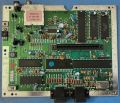
Fig. 1 - A PAL Master System II board ready for conversion. This particular revision has Sonic the Hedgehog built-in and has the Fujitsu MB3514 encoder.
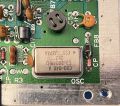
Fig. 2 - The original 53.2034 MHz oscillator...
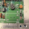
Fig. 3 - ...has been removed...
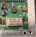
Fig. 4 - ...and a 53.693 MHz oscillator is soldered in its place.
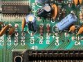
Fig. 5 - The trace connecting R10 to the original color subcarrier signal has been cut.
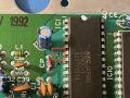
Fig. 6 - The via in front of pin 6 of the Z80 has had its solder mask scraped off and is ready to be soldered to. This via carries the CPU clock signal which will be used for the new color subcarrier.
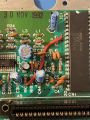
Fig. 7 - A wire has been soldered between the lower end of R10 and the Z80 clock signal.
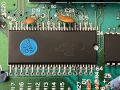
Fig. 8 - Pin 57 of the VDP, which controls video frequency, has been lifted in preparation for the next step.
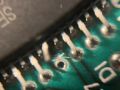
Fig. 9 - The trace which connected pin 57 to 5V has been cut, and pin 57 can then be reinserted into its via.
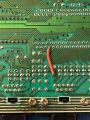
Fig. 10 - Pin 57 is now connected to ground.
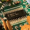
Fig. 11 - Pin 7 of the encoder has been lifted.
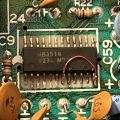
Fig. 12 - Pin 7 is now tied to pin 12 (5V) by a small piece of magnet wire.
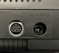
Fig. 13 - A completed conversion using a 9-pin mini-DIN connector for composite video and RGB output.


