Xbox 360:Motherboard Information: Difference between revisions
No edit summary |
|||
| Line 120: | Line 120: | ||
== Trinity== | == Trinity== | ||
Significant motherboard redesign used for the launch models of the Xbox 360 S. It combines the CPU and GPU into one 45nm chip | Significant motherboard redesign used for the launch models of the Xbox 360 S. It combines the CPU and GPU into one 45nm die while still using an eDRAM with 65nm Styx. The name of the new combied chip was Vejle, with the original codename being Valhalla. It has the same flash config as the Jasper & Tonasket and is generally quite reliable like the Jasper and Tonasket. Interestingly, non-retail developer consoles came with a "big block" 512 MB NAND instead of 64 MB. Some consoles came with an internal 4 GB Memory Unit add-on. | ||
Part Number: '''X820379''' | Part Number: '''X820379''' | ||
Revision as of 21:48, 12 April 2024
Xenon
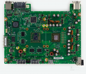
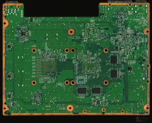
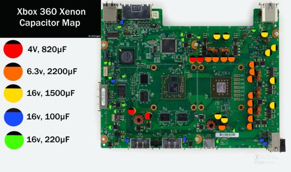
The motherboard used in beta XDKs and the finalized launch models. It has a 90nm CPU, GPU, and eDRAM. Commonly has leaky 16v 1500µF capacitors, leaky 6.3v capacitors, and unreliable GPUs. Some Xenons sent into Microsoft for RROD repair were either turned into an Elpis or received a revised 90nm Y1 GPU with high Tg underfill.
Retail Xenons came with a 16 MB NAND flash chip, whereas non-retail consoles came with a 64 MB NAND flash.
Part Number: X803600
Images
Schematics
Boardviews
Xenon (Final)
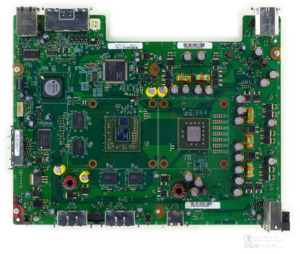
Xenon (-008 Beta XDK PCB)
Capactior Map
Elpis
Officially referbished Xenon with an Elpis GPU, which essentially a Rhea modified to work with a Xenon. These boards are known to be reliable, but still suffer from the Xenon's capacitor problem.
Part number is the same as the original Xenon.
Images
Schematics
Refer to the Xenon schematics, as they are the same PCB.
Boardview
Refer to the final Xenon boardview, as they are the same PCB.
Zephyr
Relatively significant motherboard redesign while being cheaper to manufacture and added HDMI support. It first appeared in late 2006. The encoder/analog IC (Ana) and clock generator from the Xenon were integrated in a new HANA chip. NAND Flash configuration is the same as the Xenon. The Zephyr B/C also feature CPUs with newer stepping and revised Y2/Rhea GPUs respectively. The Zephyr_B's Y2 GPU still had the original eDRAM but with a shrunken GPU die due to manufacturing optmizations, whereas the Zephyr_C's Rhea GPU had a redesigned eDRAM codenamed Stryx. The Zephyr_B first appeared in early 2007, but the Zephyr_C shortly followed around mid-2007.
Zephyr_A Part Number: X810385
Zephyr_B/C Part Number: X810387
Images
Zephyr_C
Schematics
Zephyr_A
Boardview
Zephyr_A (90nm Y1 GPU)
Zephyr_B/C (90nm Y2 or Rhea GPU)
Falcon
First motherboard to feature a 65nm Loki CPU while being slightly further simplified, like having a cheaper power delivery system (CPU Core voltage is two phases instead of three, for example). It first appeared in late 2007 consoles. Mid-2008 and later Falcons also came with reliable Rhea GPUs (came with a higher Tg underfill) and 4x128MB RAM configurations instead of the previous 8x64MB. The reliable GPUs were standardized in consoles made around June/July of 2008. NAND Flash configuration is the same as the Xenon and Zephyr.
There are also versions of this board called "Opus". They are essentially just Falcons but used as motherboard replacements for referbished Xenons. As such, they don't have an HDMI port. In fact, the AV port on the Opus was only used for it and is different from the Xenon's AV connector.
Part number: X812320
Images
Schematics
Boardview
Jasper
First motherboard to shink the GPU to the 65nm Zeus, matching with the CPU. It was first seen in late 2008 consoles. It came with an updated south bridge that supported "big block" 256 MB and 512 MB NAND flash chips with a built in user accessible memory unit, and those bigger flash chips were featured in the "Xbox 360 Arcade" retail configurations. Non-retail developer consoles with Jasper motherboards still used 64 MB NAND chips. Some Jasper motherboards produced in July 2009 also came with Kronos GPUs, which shrunk the eDRAM to also be 65nm. Some of these motherboards also came with an updated CB bootloader that patched the SMC (or "JTAG") Hack.
Most of these motherboards are known to be reliable, but some may come with leaky 16v 1500 µF Sanyo capacitors.
Part Number: X815842
Images
Schematics
Includes "Panda" integrated memory unit, using an additional NAND + USB interface as opposed to the final Jasper solution combined with main NAND.
Boardview
Tonasket
Also known as "Jasper Kronos" or by the GPU name, "Kronos". It was first spotted in late 2009 consoles. It is a minor PCB revision of the Jasper, but all of the GPUs on this board are the Kronos revision with a shrunken 65nm Stryx eDRAM. All versions of this motherboard are also known to be reliable. NAND flash configurations on the Tonasket are the same as the Jasper, except for the 256 MB config not being used anymore. All of these motherboards are patched against the SMC Hack.
This motherboard is usually referred to as the most reliable revision.
Part Number: X820379
Images
Schematics
Since the Tonasket is very similar to the Jasper, you can refer to the Jasper schematics.
Boardview
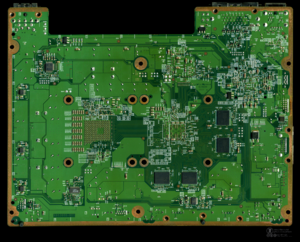
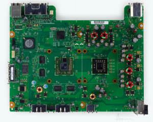
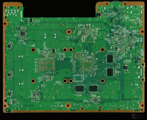
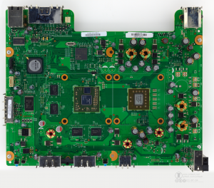
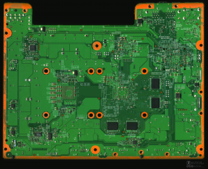
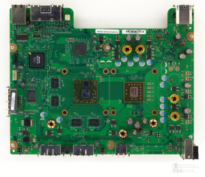
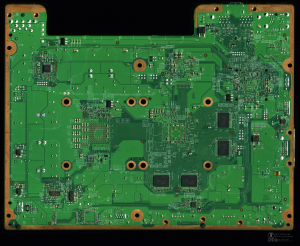
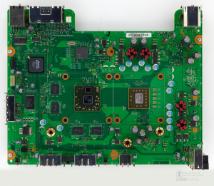
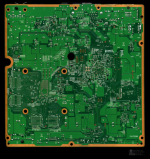
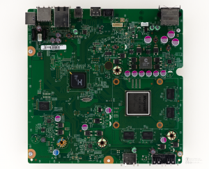
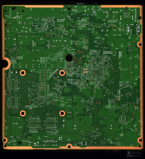
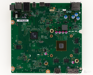
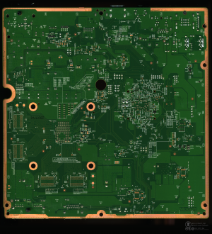
Trinity
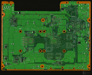
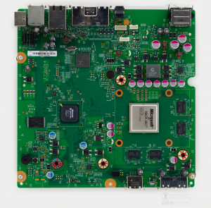
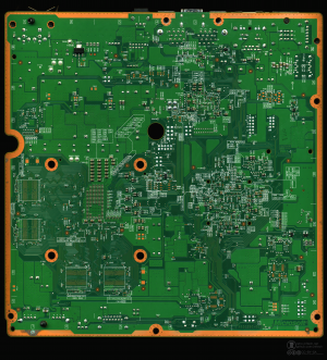
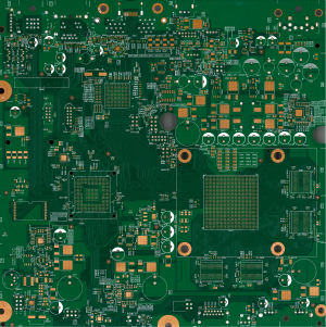
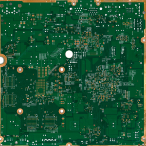
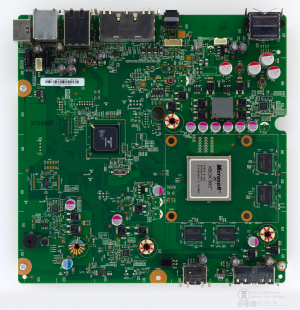
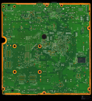
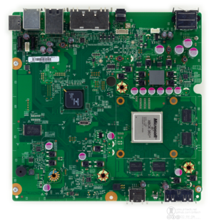
Significant motherboard redesign used for the launch models of the Xbox 360 S. It combines the CPU and GPU into one 45nm die while still using an eDRAM with 65nm Styx. The name of the new combied chip was Vejle, with the original codename being Valhalla. It has the same flash config as the Jasper & Tonasket and is generally quite reliable like the Jasper and Tonasket. Interestingly, non-retail developer consoles came with a "big block" 512 MB NAND instead of 64 MB. Some consoles came with an internal 4 GB Memory Unit add-on.
Part Number: X820379
Images
Retail
Unpopulated
Schematics
Boardview
Corona
Also known as "Corona V1 (16MB)" or "Corona V2 (4 GB)"
First appeared in mid-2011 S consoles. It has similarities to Trinity, but slightly simplified and with a new south bridge that can support on-board 4 GB NANDs. The new south bridge also integrated the ethernet PHY and HANA IC into it. It is also reliable, aside from the 4 GB flash chips.
Part Number: X857330
4 GB Build-up: X859085
Images
Corona 4 GB
Schematics
Corona PCB
Translation
Boardview
Waitsburg
Also known as "Corona V3 (16MB)" or "Corona V4 (4 GB)"
First appeared in early 2012 S consoles. POST trace for the CPU has been removed. 4 GB versions of this board also came with a BGA eMMC intead of the Hynix MMC + Phison PS700 that was previously on the Corona. It's otherwise exactly the same as the Corona.
Part Number: X862605
Images
Waitsburg 16 MB
Schematics
Since the Waitsburg is very similar to the Corona, you can refer to its schematics.
Boardview
Stingray
Also known as "Corona V5 (16MB)" or "Corona V6 (4 GB)"
Launch model Xbox 360 E motherboard. Very similar to Waitsburg but with a new power supply connector and less rear I/O. The ICs for tilt detection and front panel button chimes are also removed, but the pads are still present.
Part Number: X854326
Images
Stingray 4 GB
Schematics
Since the Stingray is very similar to the Corona, you can refer to its schematics.
Boardview
Winchester
Revised XCGPU and a vastly more simplified layout. The updated Oban XCGPU integrated the eDRAM into the main die, shrunk the manufacturing process to 32nm, and patched the "Reset Glitch Hack" by disabling many of the pins used for that exploit. This motherboard first appeared in Xbox 360 Es in late 2014.
Part Number: X879957
Images
Winchester 4 GB
| No schematics or boardviews are currently available for this motherboard. |
